Quote:
Originally Posted by MPaulHolmes

I just finally finished and submitted a basic stand-alone dual IGBT driver board, which has a 7 pin connector for +24v, ground, +5v, pwm high, pwm low, desat fault, clear desat. You can use it to drive very large IGBTs (I've tested the circuit on a 600v 600amp IGBT at 10KHz already). It Just plugs into the IGBT.
|
I think this module is going to inspire a lot of other projects.
You have done the hard bit for most people.
Well done.
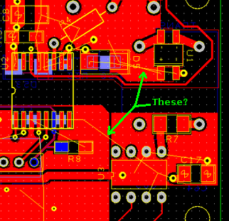
I have to ask though. On many of these layout images i keep seeing something that confuses me. I can see the components are shown for both sides and the copper traces. But then there are these thin yellow lines that seem to connect different components but sometimes they seem to stop where there are no components. Is this showing connections "as the crow flies" rather than routed? They sort of look like those Nazca lines in Peru.