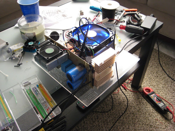
pictures!
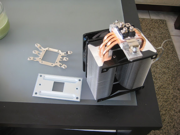
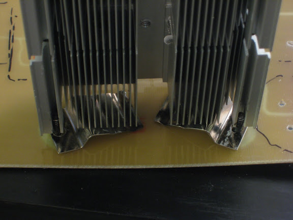
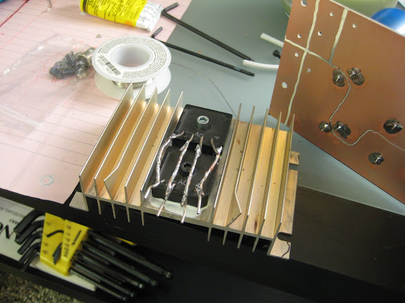
changing the mosfet mounting:
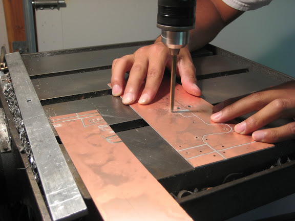
the PCB layout and the beginning cuts
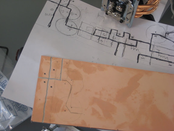
i just used a drill bit to mill away the copper and moved the board around by hand. kinda sloppy, but didn't take too long.
the completed board
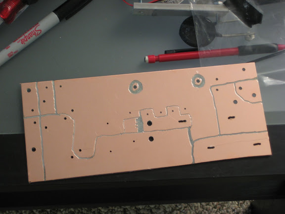
I tried to draw the components on the otherside... good thing too, cuz i actually ran into a problem with the capacitor in the top left - had to drill an extra set of holes.
the diodes in place:
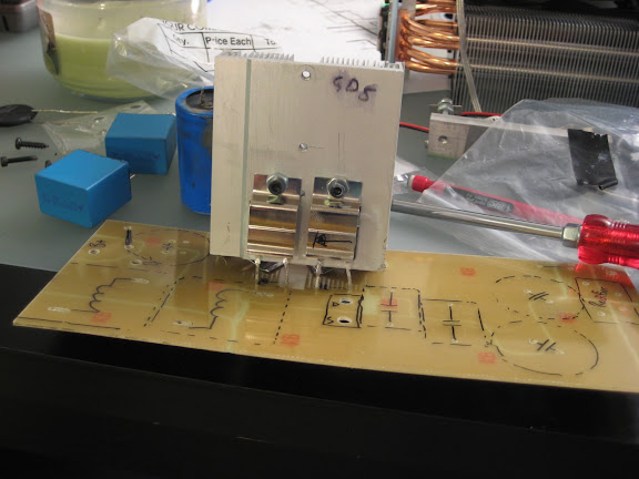
i used some mosfet clamps to spring-load the screws. prbably not the best method - it kinda bent the board.
two paralleled rectifier bridges
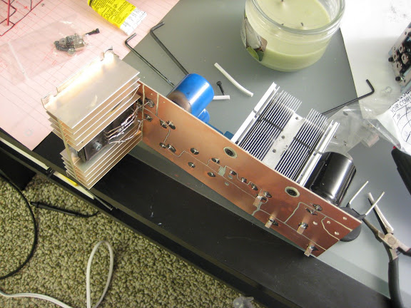
and mounted
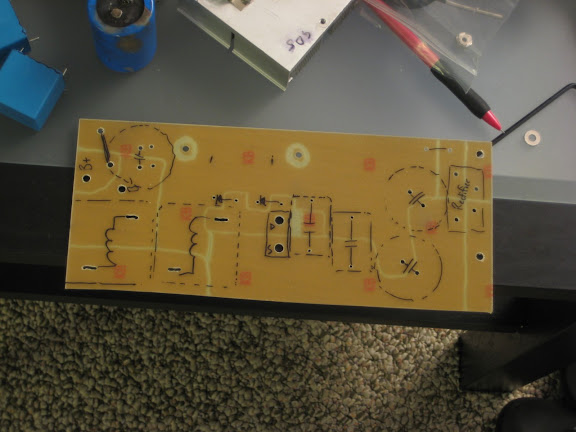
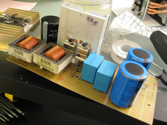
all the caps and inductors mounted. i should add that all of this mounting stuff is preliminary. now that i know the arrangement and layout seem to work, i'd probably try to figure out a better way of mounting the components so that it's not just the solder holding them in. also, I'm kind of using the pcb board as a structural member. I'm sure that isn't the best thing either...
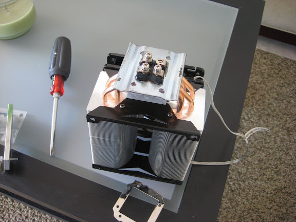
the mosfet and heatsink bolt onto the otherside. you can see the control board with two small pots that i had to turn with the yellow screwdriver. the picture had knobs.
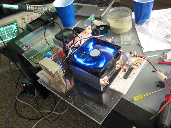
another view - if you're curious about size, the piece of plexiglass that it's on is 11x11. It'd be smaller too if it weren't for that ridiculous heatsink!