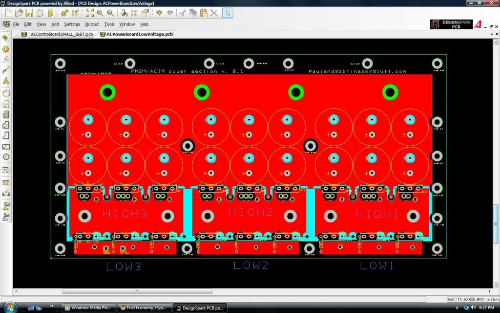
Hi Erik! I just made the power board layout without a schematic. I know that's not good practice though. Here's a picture of it:

Let's take phase 3 for example. B+ is the top plane of the board. B- is the bottom plane of the board. B+ and B- bars are on top and bottom of board respectively. Right at the top. B+ and B- share the same 4 holes. B- goes out the upper left side, and B+ goes out the upper right side. So, first you hit the bus capacitors. Then you hit the 3 high side mosfets. Then the 3 low side mosfets. The extra holes under the 3 high side mosfets are just there to add the gate resistors. They should really be on a separate board, and I"m going to make that change next time. The mosfets lay flat underneath the power board, against a base plate. I need to get some pictures of the assembly.
By the way, you are welcome to the files. I used DesignSpark, which is free, and can generate Gerber files. Oh ya, and I'm just using some LEM Hass 50-s sensors for low power tests (less than 50 amps per phase) and the higher power tests I'll use LEM Hass 300-s, which will have a limit of 300 amps per phase.